

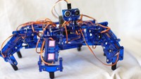


To streamline my circuitry and be more space-efficient with my designs, I etch (basic) custom circuit boards. Below I outline the necessary supplies and steps for etching.
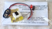
Supplies:
-Sharpies or non-water-soluble markers (optional)
-Circuit layout (digital to print on transfer paper)
-Acetone (nail polish remover)
Tools:
-Hot iron
-Tupperware or not-metal pot
-Sponges
-Good ventilation
-Latex gloves
-Hacksaw and mounting station (optional)
-Drill press and bits
-Access to a laser printer
-Scissors
-Rag or cotton balls
Steps:
Make sure to wear goggles in steps 0 and 4-6.
0. Preparations
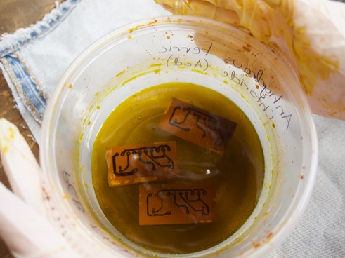
To prepare, you will want to make a hydrous ferrichloric acid by SLOWLY pouring the powder into the water! The mixture might hiss and it will heat up during the combination so be careful. This step is only necessary if the acid was bought in powder form.
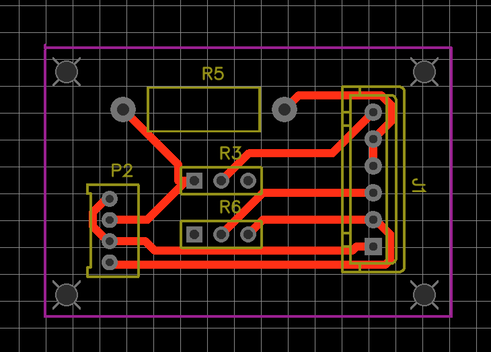
1. Making circuit
I designed a simple circuit using easyEDA.com. They have an easy-to-use system, thorough tutorials, and an expansive database of parts.
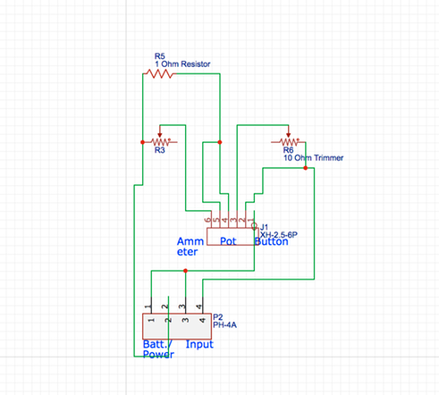
After designing the circuit, I converted it within EasyEDA to a circuit board layout. I made all of the connections on one layer (this is important - with this method, only one layer of connections is possible!)
2. Flipping and printing circuit
Next, I exported the layout in black-and-white and using built-in software on my computer I flipped the design horizontally. This is also very important since the reversed side will be copied in reverse onto the copperclad board, in turn righting the image.
Next, I sent my image to a printing shop near me (I do not have a laser printer). The reason a laser printer must be used instead of an inkjet is because laser printers work by melting a thin layer of plastic onto paper instead of ink, which will later be melted onto the copper. The shop printed on the transfer paper.
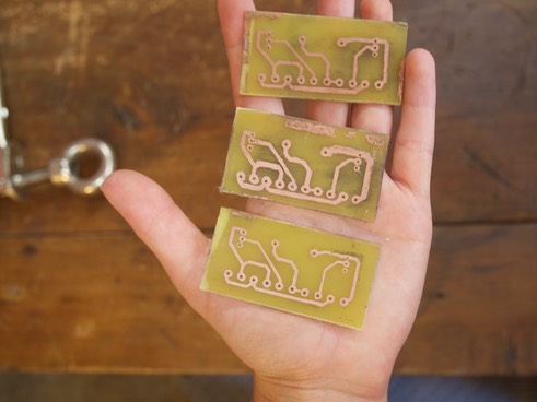
3. Cutting copperclad board and transferring reverse, cleaning
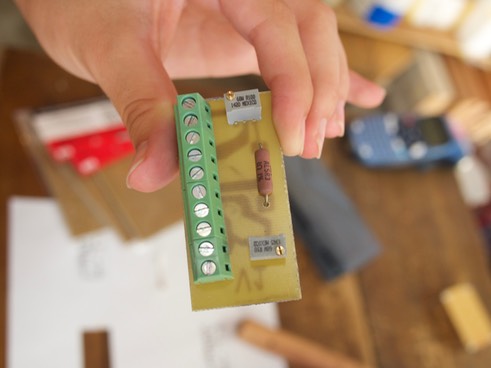
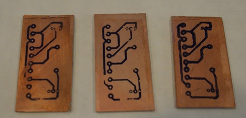
First, I cut out my circuit design from the transfer paper. Using this, I was able to estimate the approximate size of the board. I marked this using a Sharpie then I cut out the proper amount of board that I needed to make the circuit board using a hacksaw. I cleaned off the surface of the copper using acetone and a rag.
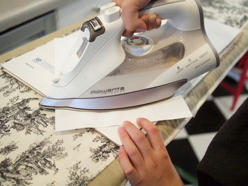
Next, I sandwiched the transfer paper (printed side down) on the copperclad board and a piece of paper on top (to prevent burning the transfer paper). I then warmed up my iron and turned off steaming and pressed down firmly until the design melted and transferred onto the copper. It took a couple trials to figure out the proper timing. Before peeling off the transfer paper, I ran the board under cold water to cool down the board and finalize the transfer. I was now ready to etch!
4. Etching board and cleaning
After preparing the ferrichloride acid solution, I was able to just drop the prepared copperclad board in. To agitate the solution in order to flush fresh acid over the surface of the board, I rocked the solution side to side and picked up the board and wiped it with a sponge that was soaked with the acid. Once there was no more copper between the circuit traces (the wires) and the yellow of the insulation was completely visible, etching was complete.
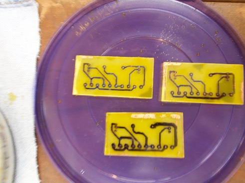
To clean off the ink from the transfer which had protected the copper during etching, I doused a rag/cottonball in acetone and swiped the surface of the board.
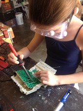
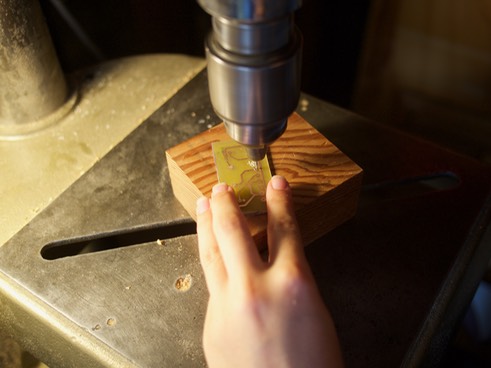
5. Drilling through-holes
Using a very thin drill bit (0.75-1.5mm) I drilled out the through-holes of the circuit allowing the mounting of through-hole parts on the other side of the board (during board population). This step is not necessary if the circuit uses only surface-mount parts.
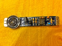
6. Using circuit board!
The circuit board is now able to be populated with parts, soldered, and generally used as a circuit board!